OKdo have partnered with Ocean Smile to provide rapid PCB prototyping services to turn your designs into production. A number of services are available, including bare PCB, PCB assembly and SMD stencils, at a low cost, with fast turnaround times.
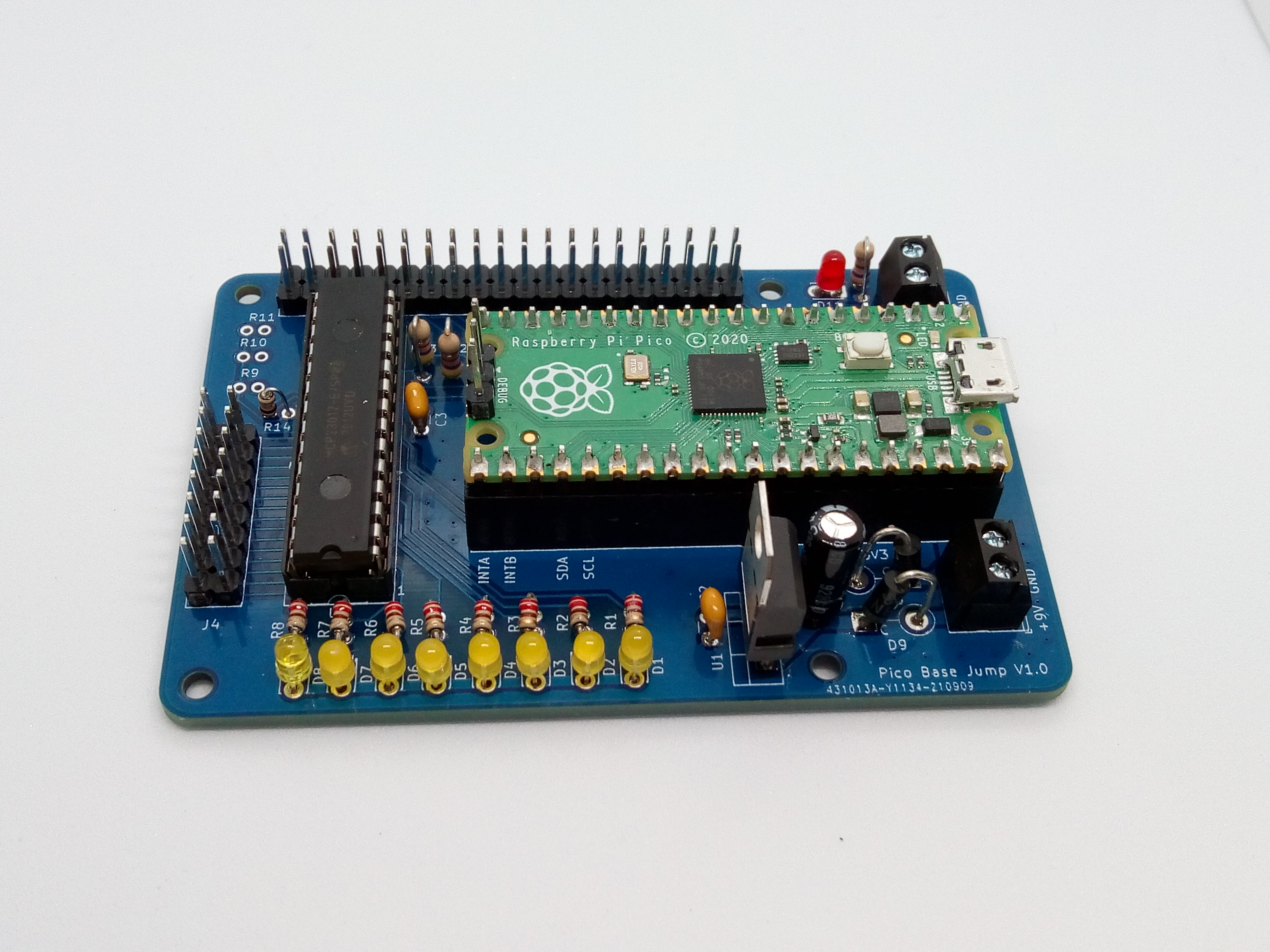
This guide takes you through the steps to design, manufacture and test a new carrier board for the Raspberry Pi Pico using the bare PCB service. The board provides a mounting point for the Pico with access to the GPIO plus power for peripherals and features a 16-bit MCP23017 port expander with LED indicators for additional input/output.
The whole project was completed using a Raspberry Pi 400 running Kicad PCB design software. Gerber file outputs were uploaded to Ocean Smile who fabricated and shipped the PCBs back in 10 days. Through-hole components were hand soldered to the PCB and the completed board was tested using C code built-in Visual Studio Code.
The PCB design, BOM, MCP23017 library and test code are open source and available on the OKdo GitHub.
1. Design
The design concept was based on being able to build the Pico into projects that use lots of buttons, switches and 5V servos, so the board could be a carrier for the Pico and a connection point for all these other ancillaries.
Power input in the range 7-12V is dropped to 5V by a linear regulator which powers the Pico and can provide up to 750mA of current to other peripherals through a separate output.
A Microchip MCP23017 16-bit I/O expander is connected to the Pico’s I2C bus giving up to 16 additional input/output connections, 8 of which have LED indicators with current limiting resistors. The MCP23017 has 2 configurable interrupts and the I2C address can be set to allow up to eight devices on the same bus, for further expansion.
The PCB outline is based on a Raspberry Pi footprint so it will fit into many commonly available cases and the Pico I/O pins are accessible on a 40-pin header. We used through-hole components so that they would be easier to solder to a bare PCB.
After considering the features of our design we built a prototype on a breadboard to test out the ideas and provide the blueprint for the PCB schematic.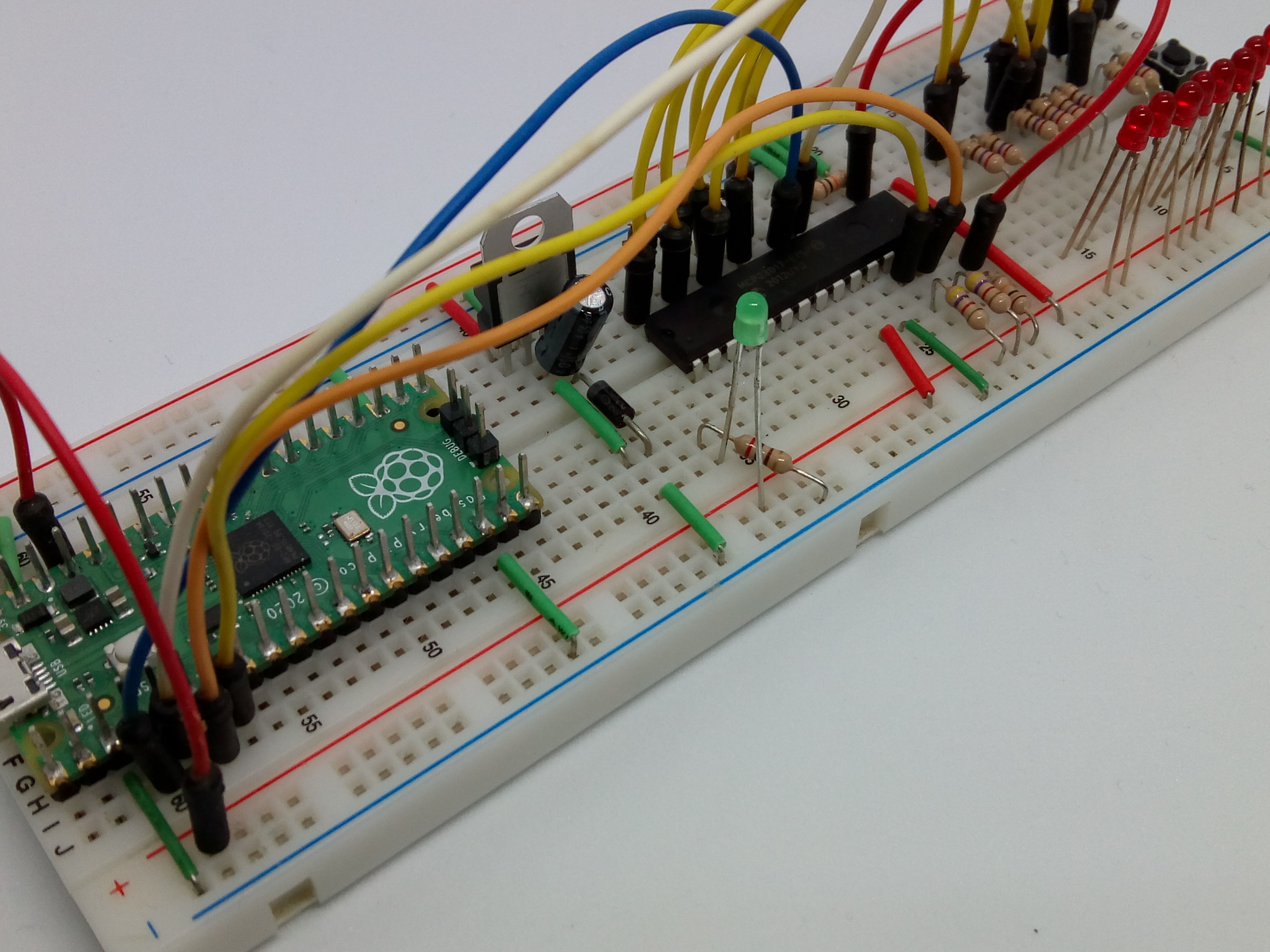
2. Software
We chose Kicad as the PCB design software because it’s open-source and runs well on the Raspberry Pi 400. There are loads of excellent YouTube videos and tutorials produced by Kicad and others, making it easier to learn how to design PCBs. Kicad has a large library of common components that can be used in the PCB design, simplifying the process for beginners.
Installation is simple as Kicad is in the Raspberry Pi OS repo. We used version 5.1.4 by executing the following commands in the terminal:
sudo apt update
sudo apt upgrade
sudo apt install kicad
Developing the C library for the MCP23017 and the test programs to run on the Pico was done using Visual Studio Code. Full installation details for this are in a separate guide here.
The full Kicad schematics and layout files along with the C library and test code is available in the OKdo GitHub.
3. Schematic
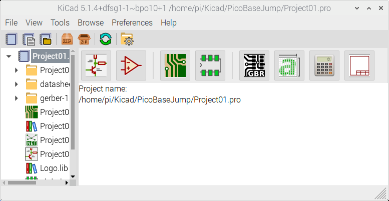
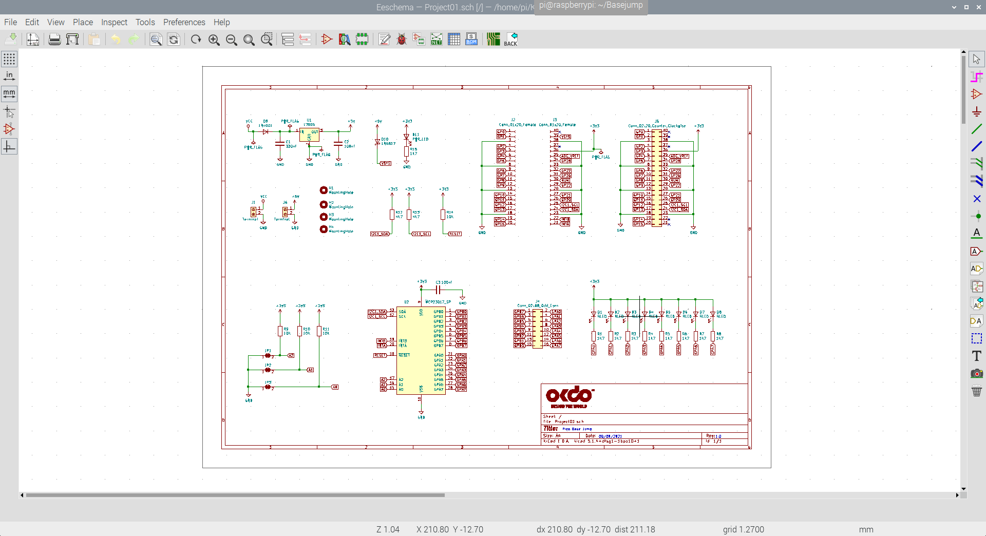
After creating a New Project in Kicad, the first step is to create a schematic diagram of the circuit. This represents all the components used in the design and their electrical connections to one another.
It is easiest to create a logical view of the circuit rather than trying to join all the components together with connections in the schematic.
We started by designing the power supply section by placing the 5V linear power supply and its decoupling capacitors using the Symbol tool and then connecting the parts with the Wire tool. Connections to GND and Power can be made by attaching power symbols. The L7805 part datasheet contains all the specific details, so it’s a matter of just transferring these to your diagram.
We used two Female Header symbols to represent connections to the Pico itself and used Global Labels for the GPIO, Power and I2C connections to a 40-pin connector and the MCP23017.
The Kicad symbol library contains the MCP23017 symbol so this can be placed and I2C and interrupt pins connected to the Pico header. The GPIO connections go to another 16-pin male header for ports A & B on the device. VCC for the MCP23017 is supplied from the Pico’s 3V output.
8 LED’s and their current limiting resistors were added using Global Labels for the MCP23017 connections, pulling them up to +3V.
Solder Jumpers were placed connected to GND and 10K pull-ups, which are not fitted. This externally biases the MCP23017 and gives it an I2C address of 0x20 Hex. Cutting the jumpers and fitting the resistors allows the address to be changed if required.
We also added pull-up resistors for the I2C bus and a Schottky diode to prevent reverse powering of the circuit if both the external supply and Pico USB connections are connected at the same time. There is also a power indicator LED, screw terminals for the external power and mounting holes for the PCB.
Once all these components symbols were placed and connected, a Design Rule check was performed. This ensures that everything is properly connected. Any issues were fixed before moving on to the layout stage.
Attaching special Power Flag symbols to VCC and GND allows the Design Rules check to pass
Each component symbol represents an electrical view of the part but before you can proceed to PCB layout, each symbol needs associating with a physical footprint representing solder pads. For example, the MCP23017 is available in both through-hole and surface mount packages so there are several footprints to choose from. The Footprint Assignment tool is used to create this link. Kicad has many of the standard package footprints already in its library but if there isn’t one for a particular part, it’s possible to create one using the Footprint Editor tool.
The Netlist tool was then used to create a netlist which is saved as a file.
Finally, the PCBNew tool generates a PCB Layout from the schematic. We kept the default board settings of 1.6mm thickness and double-sided PCB.
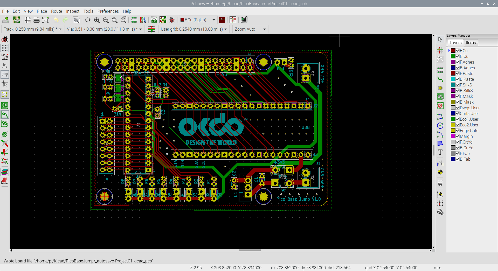
4. Layout
The PCB Layout is the physical representation of your design and is where you position your component footprints onto the PCB outline and connect them together.
The PCBNew tool generates a starting point for the layout and dumps all the footprints down with connecting lines called a “Rats Nest”. From there you can click and drag individual components into position in your layout.
We started by creating the board outline according to the Raspberry Pi physical dimensions given in its datasheet. We then positioned the mounting holes and locked them so they couldn’t be moved accidentally. The Measuring tool was used to get a very accurate location of each hole with one of them acting as a datum point.
Pico headers were then positioned and accurately measured before locking in place, followed by the Pico’s GPIO connector, the MCP23017 footprint and the associated connectors all placed approximately.
The power supply circuitry was placed next along with its supporting components and the power output. This left just about enough room to locate all the LED’s, decoupling capacitors and pull-ups.
Once all the components are positioned it’s time to create the connecting traces. We started by laying out the 5V and 3V power traces which we increased in width from the default settings. All other settings were left as Kicad defaults.
Where possible we tried to keep traces on the top layer but the 3V line, some of the 5V line and the solder jumpers were placed on the bottom layer.
The fiddly process of connecting all the remaining components then took place, threading the traces between the connector pads. This gets more and more difficult as you near completion in this space-constrained board. A few traces were run on the bottom layer to complete this.
A top and bottom layer ground pour was created using the Filled Zone tool to complete the process then a few vias were added using the Vias tool to stitch the ground planes together in areas where there were no through holes.
The finishing touch was to add a logo created from a bitmapped image using the Bitmap to Component tool on the silkscreen layer.
After a final Design Rule check on the layout, the PCB was ready for fabrication.
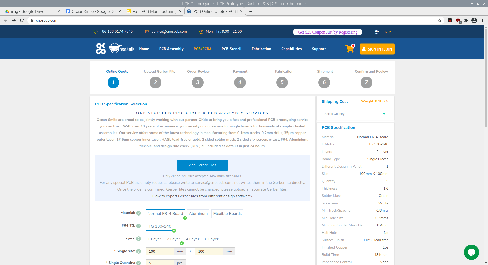
5. Fabrication
Following the link to PCB Prototyping from the OKdo site leads to the Ocean Smile fabrication workflow, where you can create an account and start the fabrication process by obtaining a quotation for your design.
The first stage is to set the fabrication parameters for your PCB on the form. We left all the settings as their defaults as they are compatible with the Kicad settings, except for the Surface Finish. This was set to HASL Lead-Free. You can then see the cost of your board, excluding shipping charges which are added later.
Ocean Smile has a link to very clear step by step instructions for generating Gerber files from various popular PCB design packages, including Kicad and we followed these to produce the fabrication output files using the Plot function in the PCB Layout view. The exported files were all placed into a .zip file and uploaded to Ocean Smile.
The order then goes through an automated review and if it passes, payment can be made for fabrication and shipping to your address. You can then follow the progress of your order online and a tracking number is issued when the PCB is shipped. The whole process took 10 days, including shipping to the UK.
6. PCB build
Once the PCBs were received, the build process could commence.
Initially, the bare PCB was checked for continuity with a multimeter and by referencing the schematic and layout in Kicad. We found everything to be as expected which was a great start.
It’s useful to build up the first board in stages so that any issues are easier to isolate. So we started by soldering the power supply components and used a bench power supply to test that we had 5V where expected. Again, everything worked perfectly.
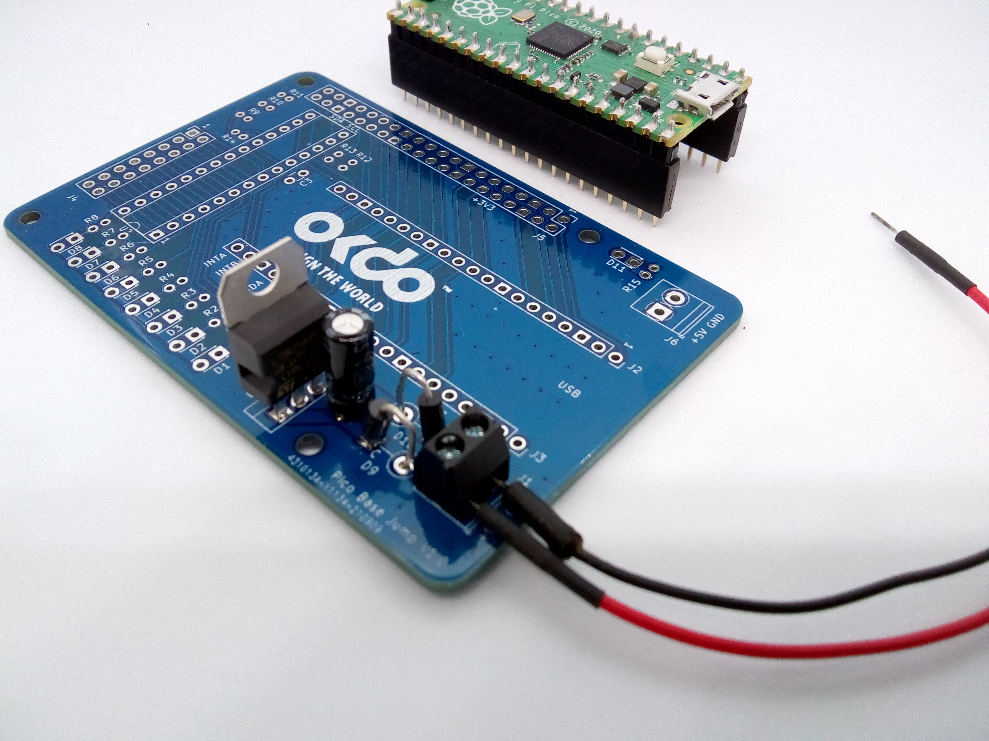
We then added the Pico headers, mounted it and tested that we could program the Blink code from the Pico examples. This worked fine so we went ahead and soldered on the MCP23017 and remaining components ready for final testing.
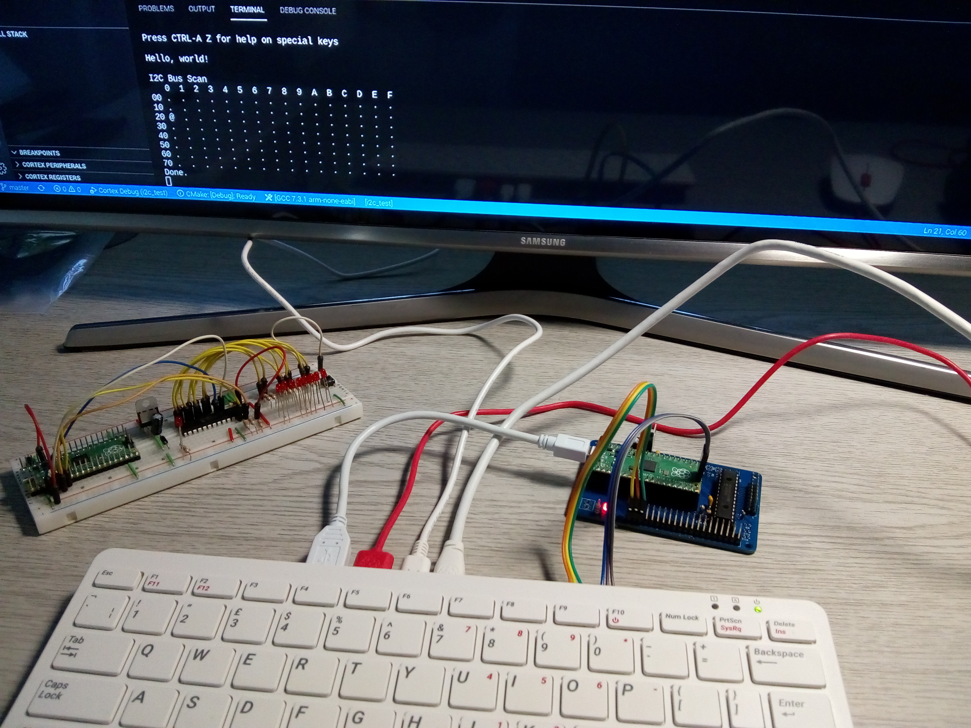
7. Testing
To give the board a thorough workout we connected up a bank of push buttons to the MCP23017 GPIO headers on bank B then wrote a small library for the MCP23017 and some test code in C using Visual Studio Code.
The Pico SDK has great support for I2C devices and provides example code for reading and writing to I2C device registers detailed in the MCP23017 datasheet. There’s also an example of using interrupts with the Pico GPIO to act as a reference.
All the code we used is available in the OKdo Github and can be installed on your Pi by cloning it from the repo.
The first test scans the I2C bus for devices to check if the MCP23017 is connected to the Pico. The default address for the board is 0x20 Hex and that test passed.
Next, we polled the MCP23017 GPIO on bank B to listen for button presses. The GPIO input can be read in a single byte and then used to set the GPIO output on Bank A, which is connected to the LED indicators. So that when a button is pressed, the corresponding LED turns on, and when it’s released it switches off again. This test passed as well.
The final check was to check the interrupts function. The MCP23017 has interrupt outputs that can be set to trigger when the GPIO changes state. We used the same button circuit but configured interrupts on the Pico’s GPIO to detect the MCP23017 interrupt line on bank B whenever a switch was pressed. The interrupt register contains the button states which were then used to set the corresponding LED states. Reading the interrupt clears it, so it’s ready to fire again. This final test also passed with flying colours!
Summary
This guide has given an overview of all the steps needed to take a circuit design from concept to a working PCB prototype. From building a test circuit, creating a schematic and layout in Kicad, producing Gerber file outputs and uploading to Ocean Smile and finally building the fabricated PCBs and testing them with C code running on the Pico.
The Ocean Smile PCB fabrication service was very easy to use and was well supported for customers using Kicad to design their boards. We were also pleased to report that our design worked first time and as specified in our order.
All the design and coding was done using a Raspberry Pi 400 and Open Source software making the manufacture of PCBs very accessible at a very low cost.
We now have a cool new board for our Pico projects to make connecting buttons, servos and other devices much easier and we hope this will inspire you to go ahead and create your own PCBs.
Happy fabricating!
Like what you read? Why not show your appreciation by giving some love.
From a quick tap to smashing that love button and show how much you enjoyed this project.

